/
The company believes it’s more than two years ahead of TSMC and Samsung in backside power delivery.
Share this story
:format(webp)/cdn.vox-cdn.com/uploads/chorus_asset/file/24703490/Intel_PowerVia.jpg)
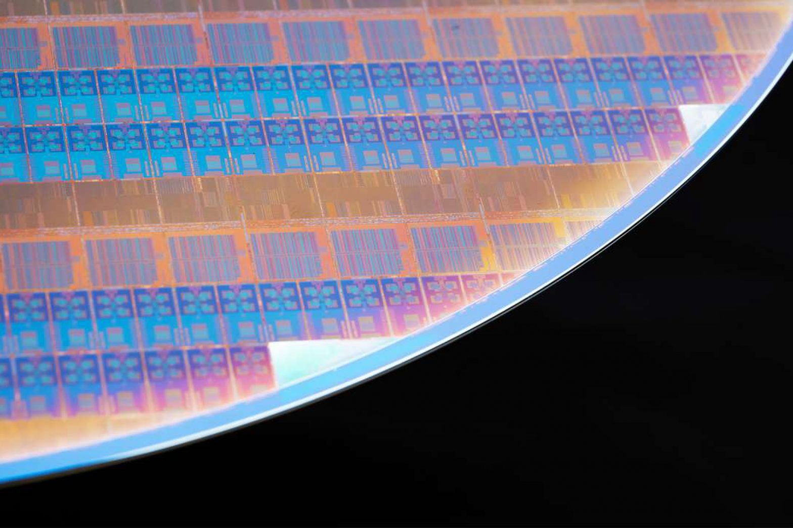
After years of struggling to make good on its chipmaking promises, Intel is publishing two papers at next week’s VLSI Symposium detailing a new way to build chip nodes that should make for more efficient processors, according to its press release today. It’s called PowerVia, and if Intel pulls this off, it’s a pretty big deal in the race to make smaller and smaller processor nodes.
PowerVia would be crucial for making the smaller, less power-hungry chips that are part of Intel’s road map debuted in 2021. It would move all power rails to the back of the chip, bringing power directly to the components that need it instead of routing it around the side and up into an “increasingly chaotic web,” to borrow Intel’s phrasing, of layered power and signal wires, as is done now.
The benefit of this new method is power and signal wires have more space and can therefore be bigger and more conductive.
Intel says it proved out the solution with a test chip called Blue Sky Creek, based on an efficient core it will be putting in its forthcoming Meteor Lake PC processor. It says the new method allows for both better power delivery and better signal wiring.
The VLSI 2023 Twitter account tweeted a couple of pictures from one of Intel’s papers on June 2nd, one of which was done with thermal imaging.
Intel expects its new PowerVia solution to be ready to be added to manufacturing in 2024. Per its road map, it expects its new process will help it regain ground it’s lost over the last few years, as rivals like AMD and TSMC have made more powerful and more efficient processors.
A write-up in AnandTech puts a lot of Intel’s work to get here in context, discussing in detail the challenges the company faces with the new design. Per the article, it would put Intel at least two years ahead of its competitors when it comes to actually producing chips with this new technique.
